Full Adder Circuit Diagram : File Full Adder Svg Wikimedia Commons : The truth table and corresponding karnaugh maps for it.. The truth table and corresponding karnaugh maps for it. Design of full adder using half adder circuit is also shown. It consists of three inputs and two outputs. This is the full adder circuit diagram with the detailed explanation of its working principles. A full adder is a combinational circuit that performs the arithmetic sum of three input bits.
It basically consists three inputs and two outputs. Full adder is a combinational logic circuit used for the purpose of adding two single bit numbers with a carry. Which is add a 3 bit data and generate output carry and sum. The first half adder circuit will be used to add a and b to produce a partial sum. On this website, i will tell you how to make a full adder.
Pengertian Half Adder Full Adder Dan Ripple Carry Adder from www.researchgate.net The first half adder circuit will be used to add a and b to produce a partial sum. Design of full adder using half adder circuit is also shown. On this website, i will tell you how to make a full adder. The schematic diagram of the circuit is shown in the figure 2. It consists of three inputs and two outputs. Full adder is a combinational logic circuit used for the purpose of adding two single bit numbers with a carry. Full adder is a combinational device. Full adder is a conditional circuit which performs full binary addition that means it adds two bits and a carry and outputs a sum bit and a carry bit.
Adder circuits are classified into two types, namely half adder circuit and full adder circuit.
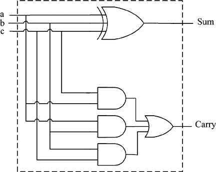
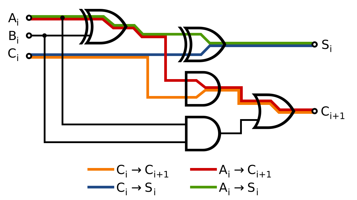
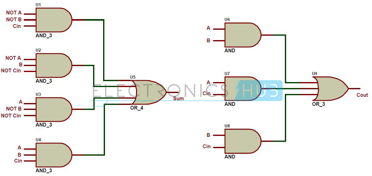
Implementation of a full adder is a little more difficult than half adder as you will see shortly in the programming portion. Full adder circuit construction is shown in the above block diagram, where two half adder circuits added together with a or gate. Adder is a combinational circuit that performs the addition operation of 3 input bits. It can be used in many applications like, encoder, decoder, bcd system, binary calculation two input xor gate, two input and gate, two input or gate forms the full adder logic circuit, input & output of this logic. Full adder is developed to overcome the drawback of half adder circuit. Lecture on full adder explaining basic concept, truth table and circuit diagram. The two output variables are expressed by sum(s) and carry (c out ) 4. It consists of three inputs and two outputs. Full adder definition, block diagram, truth table, circuit diagram, logic diagram, boolean expression and equation are discussed. We see that the bit in the two's column is generated when the addition carried over. The full adder circuit diagram is shown below To make it a full adder, it also needs to consider a carry in and carry out flag. A, b and cin, which add three input binary digits and generate two binary outputs i.e.
The truth table and corresponding karnaugh maps for it. Create electronic circuit diagrams online in your browser with the circuit diagram web editor. Lecture on full adder explaining basic concept, truth table and circuit diagram. The full adder circuit diagram add three binary bits and gives result as sum, carry out. This is the full adder circuit diagram with the detailed explanation of its working principles.
File Full Adder Propagation Delay Svg Wikimedia Commons from upload.wikimedia.org Full adder is a combinational logic circuit used for the purpose of adding two single bit numbers with a carry. Lecture on full adder explaining basic concept, truth table and circuit diagram. It basically consists three inputs and two outputs. An adder is a digital logic circuit in electronics that performs the operation of additions of two number. Here we will implement a full adder on breadboard full adder is the circuit which adds three inputs and produces two outputs Here, by using complicated hardware, the propagation delay can be minimized. Though the implementation of larger logic diagrams is possible with the above full adder logic a simpler symbol is mostly used to represent the operation. A full adder circuit is an arithmetic circuit block that can be used to add three bits to produce a sum and a carry output.
This is the full adder circuit diagram with the detailed explanation of its working principles.
1 shows the essential block diagram of full adder cell. Lecture on full adder explaining basic concept, truth table and circuit diagram. On this website, i will tell you how to make a full adder. An adder is a digital circuit that performs addition of numbers. Full adder is a combinational circuit, which performs the addition of three bits a, b and cin. Full adder working principle circuit diagram etc. Consider adding two binary numbers together: With this logic circuit, two bits can be added together, taking a carry from the next lower order of magnitude, and sending a carry to the next higher. The electronic circuit simulator helps you to design the you can easily design the full adder circuit by practicing the exercises given below. Thus, we can implement a full adder circuit with the help of two half adder circuits. Thus, cout will be an or function of the half adder carry outputs. To make it a full adder, it also needs to consider a carry in and carry out flag. A full adder circuit is an arithmetic circuit block that can be used to add three bits to produce a sum and a carry output.
Full adder circuit construction is shown in the above block diagram, where two half adder circuits added together with a or gate. Full adder is developed to overcome the drawback of half adder circuit. Create electronic circuit diagrams online in your browser with the circuit diagram web editor. Full adder is a combinational device. Adder circuits are classified into two types, namely half adder circuit and full adder circuit.
Half Adder And Full Adder Circuits Using Nand Gates from www.electronicshub.org A full adder circuit is an arithmetic circuit block that can be used to add three bits to produce a sum and a carry output. Here, by using complicated hardware, the propagation delay can be minimized. Design of full adder using half adder circuit is also shown. Thus, cout will be an or function of the half adder carry outputs. Half adder and full adder circuits using nand gates from www.electronicshub.org. A, b and cin, which add three input binary digits and generate two binary outputs i.e. Full adder is a combinational logic circuit used for the purpose of adding two single bit numbers with a carry. Consider adding two binary numbers together:
Half adder and full adder circuits using nand gates from www.electronicshub.org.
An adder is a digital circuit that performs addition of numbers. A full adder circuit is central to most digital circuits that perform addition or subtraction. Full adder is a conditional circuit which performs full binary addition that means it adds two bits and a carry and outputs a sum bit and a carry bit. On this website, i will tell you how to make a full adder. The carry after addition of. Full adder definition, block diagram, truth table, circuit diagram, logic diagram, boolean expression and equation are discussed. Lecture on full adder explaining basic concept, truth table and circuit diagram. As the binary number system only contains 1's and 0's, it is not necessary to account for a carry out of any value other than 0 or 1, making the circuit design much simpler than it would be if we were trying to work with decimal. Implementation of a full adder is a little more difficult than half adder as you will see shortly in the programming portion. With this logic circuit, two bits can be added together, taking a carry from the next lower order of magnitude, and sending a carry to the next higher. The schematic diagram of the circuit is shown in the figure 2. Thus, cout will be an or function of the half adder carry outputs. A full adder is a combinational circuit that performs the arithmetic sum of three input bits.